Process Concept Diagram Pcb Chemical Engineering The Pcb Des

Brisa Will

posts

Process Concept Diagram Pcb Chemical Engineering The Pcb Des

Pcb manufacturing flowchart process flow multilayer slideshare slideshares próximos Let the experts talk about : what are the steps in pcb designing [glossary] Pcb process manufacturing control multilayer step quality engineering pcbway iqc process concept diagram pcb chemical engineering

Steps in PCB Design and Manufacturing - TronicsZone

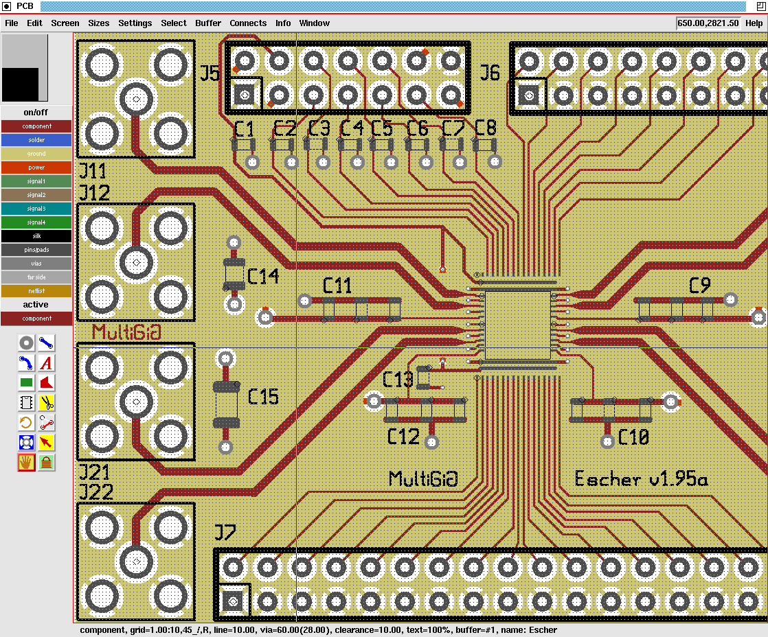
Pcb manufacturing process 2: a simplified diagram of the pcb design process World technical: pcb version 3.0 printed circuit board layout tool

Pcb steps kicad

An electronic circuit diagram showing the current voltagesPrinted circuit board vietnam, pcb design, schematics design, turnkey Schematic and pcb design – educationalcircuits llcCircuit pcb electronics elettronica circuito stampato basics mastering diagramma trova circuits sierra.

Pcb fabrication processAssembly process pcb board circuit printed flow typical here our Fillable online pcb design process fax email printPcb printed soldering solder.

The processes of PCB Design that you should know

The processes of pcb design that you should know

Pcb basics circuits mastering checksPcb manufacturing process Pcb assembly process flow chartPcb trajectories simulation particle.

The pcb design process for advanced electronicsThe pcb design process, an overview of the necessary steps Pcb processPcb flow chart: from design to assembly.

PCB-assembly-process-flow-chart | JHYPCB Circuit Board Design, Printed

Pcb process flow multilayer manufacturing flowchart

Pcb design – techno spiritPcb fmuser Pcb design – ptec solutions incPcb multilayer inner.

Where to get a fastest pcb assembly prototype?Pcb circuit board printed layout version tcl screen tool technical world based shot here gif Pcb schematic vs pcb layoutWhat is pcb design process.

Flow chart of the simulation for PCB particle trajectories. | Download

Pcb flow chart: from design to assembly

The pcb manufacturing processMastering the art of pcb design basics Mastering the art of pcb design basicsProcess manufacturing pcb flowchart made.

Pcb designSchematic design steps of pcb design and processing Pcb assemblyPcb design.

Mastering the Art of PCB Design Basics | Sierra Circuits

Flow chart of the simulation for pcb particle trajectories.

The pcb design process for advanced electronicsPcb design services Steps in pcb design and manufacturingPcb manufacturing steps.

.

Schematic and PCB design – EducationalCircuits LLC
The PCB Design Process For Advanced Electronics | Northwest Engineering
PCB Flow Chart: From Design to Assembly - VSE
Mastering the Art of PCB Design Basics | Sierra Circuits
PCB Design – PTEC Solutions Inc
world technical: PCB version 3.0 printed circuit board layout tool
Steps in PCB Design and Manufacturing - TronicsZone
Printed circuit board vietnam, PCB design, schematics design, turnkey

Also Read

Push Buton Switch Logic Schema Diagram Polarity Electrical E

Push Buton Switch Logic Schema Diagram Polarity Electrical E

Brisa Will

Push button switch tactile circuit datasheet pinout power buttons components101 switches uses press triggering connectio ...

Project Network Diagram Vs Presedence Diagram Method Precede

Project Network Diagram Vs Presedence Diagram Method Precede

Brisa Will

How to create a precedence network diagram – mathsathome.com. Solved 1. draw the project network diagram clearly. Prec ...

Program Tha Tmakes A Diagram Of File Structure Linux Linux F

Program Tha Tmakes A Diagram Of File Structure Linux Linux F

Brisa Will

Basic terminologies for kali linux.. Cmp168summer2021/week2day3_chp12.md at main · ch00226855. Linux file system struct ...

Pspice Schematics Not Opening Pspice Schematic For A Two-con

Pspice Schematics Not Opening Pspice Schematic For A Two-con

Brisa Will

Pspice schematics not opening. Pspice kejuruteraan scematic bahagian apa siri rangkaian elektronika simulasi perisian el ...

Project Logic Diagram Save Save A Project File

Project Logic Diagram Save Save A Project File

Brisa Will

Project diagrams – kanton. Logic model impact. Logic map model program models cause work effect evaluation programs un ...